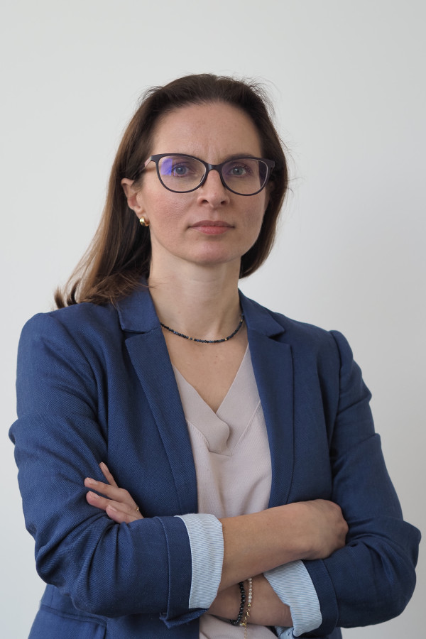
Team Leader
Research topics
The Laboratory of Semiconductor Characterization is part of the Institute of High Pressure Physics at the Polish Academy of Sciences. Using a variety of research methods, such as electron microscopy, X-ray diffraction, deep level transient spectroscopy (DLTS), atomic force microscopy, and secondary ion mass spectrometry (SIMS), we characterize crystals and epitaxial layers of semiconductors, as well as other materials. These techniques provide information about the structural quality of the materials under study and enable the identification of defects.
Team Leader
Team Members
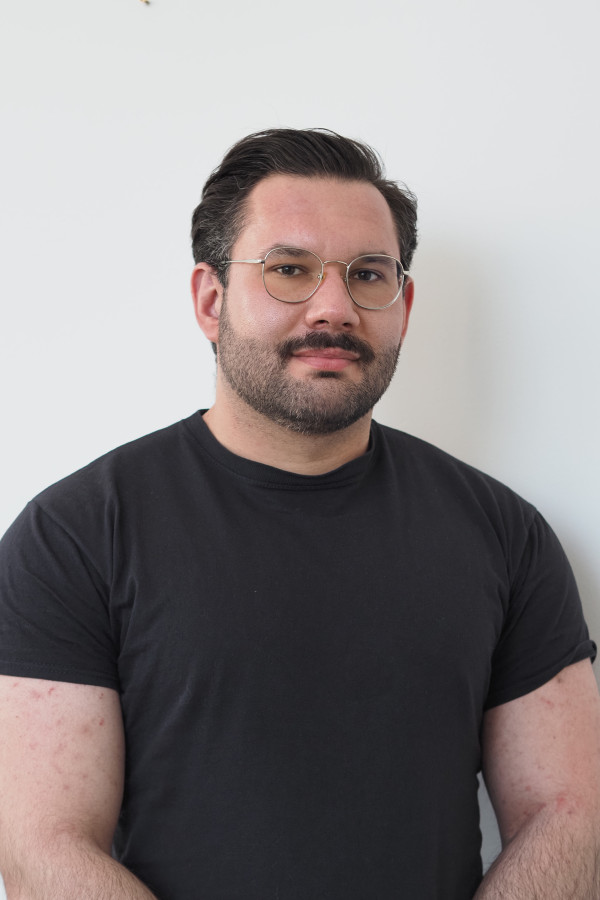
Research Assistant
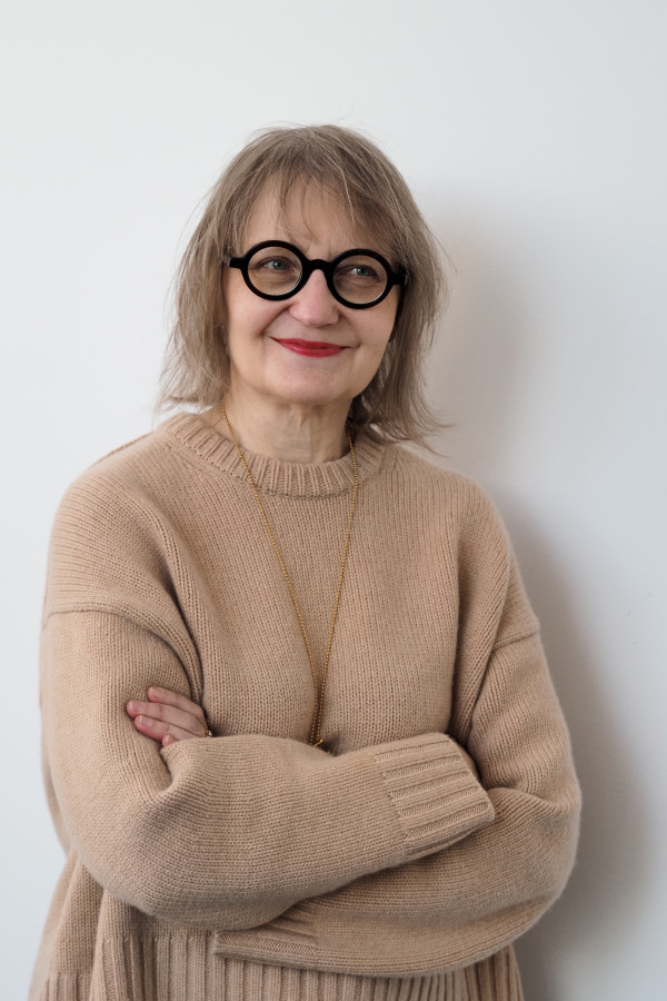
Research Assistant
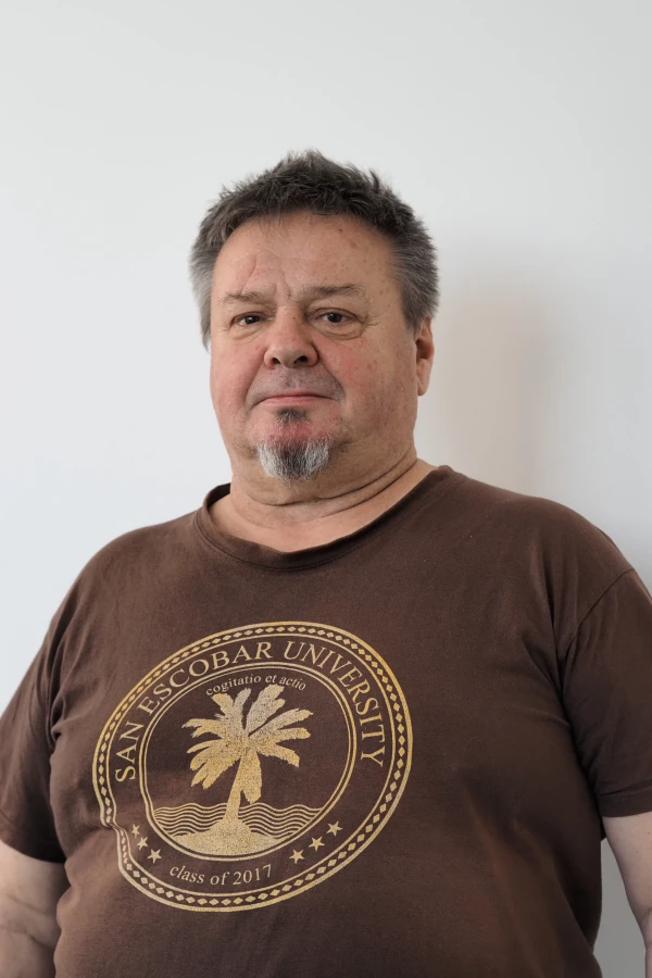
Technician

Technician
Assistant Professor
Assistant Professor
Professor
Assistant Professor
Assistant Professor
News
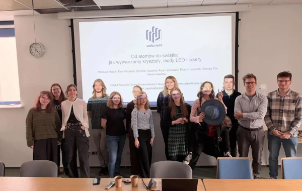
 02/10/2026
"ProbUWka" Chemistry Student Science Club visited Institute of High Pressures Physics
 09/09/2026
DRIP21 conference summary. Prof. Julita Smalc-Koziorowska was appointed as a Chair of International Steering Committee
 04/09/2026
XI Winter Workshop on physics and application of nitride semiconductors - save the date!
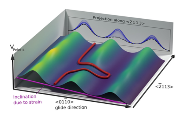 25/06/2026
We learned how do dislocations with large Burgers vectors move in InGaN/GaN material system
 12/06/2026
Five NCN grants for IHPP PAS researchers in OPUS 30 and SONATA 21 calls
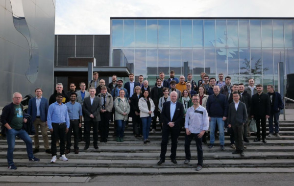 25/05/2026
IHPP PAS at the 2nd Finnish-Polish Symposium on Nitride Semiconductor Science and Technology in Helsinki
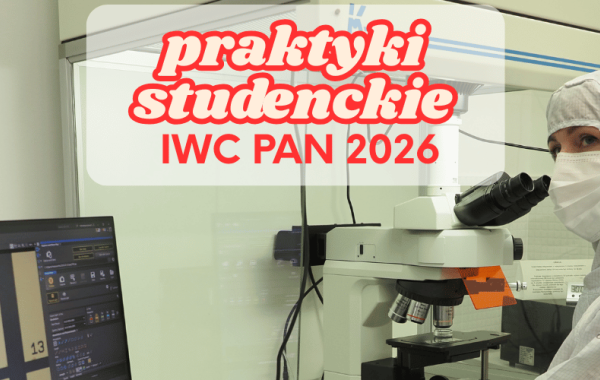 15/05/2026
Praktyki wakacyjne w IWC PAN
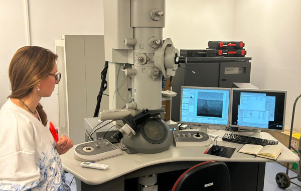 30/04/2026
The profession of a scientist and the GaN crystal properties
 03/02/2026
Call for abstracts – DRIP21
Ongoing Projects
 Artur Lachowski
-
 August 2025
August 2028
August 2025
August 2028
- Michał Leszczyński
-
April 2025
March 2028
- Michał Leszczyński
-
June 2023
June 2027
- Grzegorz Staszczak
 National Science Center
-
January 2022
January 2027
- Robert Czernecki
- National Science Center
-
January 2022
January 2027
Completed Projects
- Julita Smalc-Koziorowska
- National Science Center
-
December 2021
June 2026
- Ewa Grzanka
-
January 2022
January 2026
- Joanna Moneta
- National Science Center
-
August 2024
August 2025
- Piotr Kruszewski
- National Science Center
-
January 2021
April 2025
- Michał Leszczyński
- Narodowe Centrum Nauki
-
January 2020
January 2025
- Michał Leszczyński
- National Science Center
-
February 2020
May 2024
- Michał Leszczyński
- National Science Center
-
January 2019
December 2023
- Robert Czernecki
- National Center for Research and Development
-
November 2019
October 2023
- Michał Leszczyński
- Narodowe Centrum Badań i Rozwoju
-
September 2020
July 2023
- Monika Masłyk
- National Science Center
-
October 2021
February 2023
- Julita Smalc-Koziorowska
- Narodowe Centrum Nauki
-
March 2017
March 2022
- Michał Leszczyński
- Foundation for Polish Science
-
September 2017
May 2021
Equipment
Fabrication of materials and structures
Fabrication of materials and structures
Fabrication of materials and structures
Sample preparation for transmission electron microscopy (TEM)
Characterization of materials and devices
FEI Tecnai G2 F20 S-TWIN Transmission Electron Microscope (200 kV)
Characterization of materials and devices
Characterization of materials and devices
Characterization of materials and devices
Characterization of materials and devices