MBE Laboratory
Institute of High Pressure Physics PAS
About us
MBE research group is a part of the Institute of High Pressure Physics Polish Academy of Sciences (IHPP PAS) "Unipress".
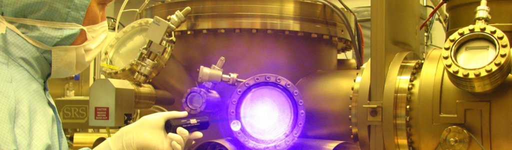
We focus on the development of blue and green light-emitting diodes (LEDs) and laser diodes (LDs) using plasma-assisted molecular beam epitaxy (PAMBE). We carry out the research on long-wavelength light emitters: implement improvements in structure design and optimize optical and electrical parameters of gallium nitride (GaN) based devices. We investigate crystal growth mechanisms on GaN surfaces of various polarity and crystallographic orientation. We fabricate and study nitride heterostructures with tunnel junction. We also study vertical heterojunction transistors n-p-n (GaN/InGaN/GaN) fabricated on GaN substrates using MBE.
Highlights
Bidirectional LEDs live on Polskie Radio Trójka
January 4, 2024 live on Polskie Radio Trójka Mikołaj Żak from our Institute (MBE Laboratory) presented a new look at LEDs that can operate efficiently with alternating current power . It was a commentary on a recently published work in Nature Communications, which is reported by the website [Naukawpolsce.pl](https://naukawpolsce.pl/aktualnosci/ news%2C99998%2CPolish-idea-for-bidirectional-LEDs-without-power-acdc.html). We invite you to visit the portal website.
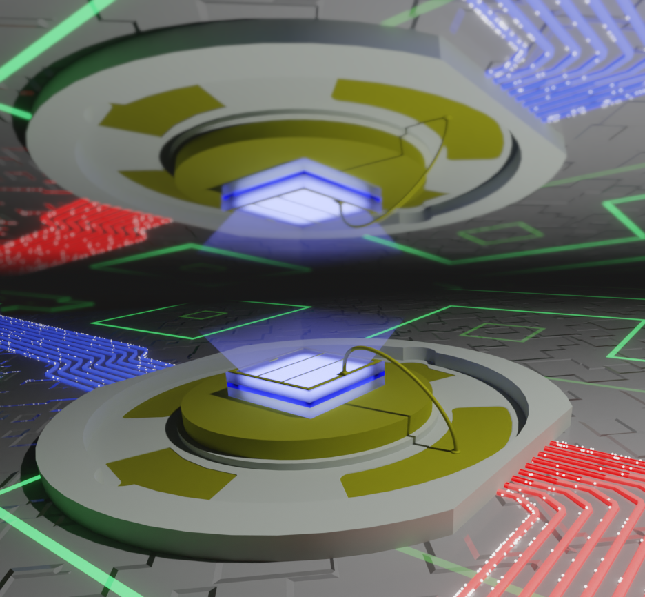
Fig. Visualization of the operation of a bidirectional diode. Author: Mateusz Hajdel (IWC PAN), co-author of the article.
Focus.pl also writes about bidirectional diodes developed by Mikołaj Żak
Lately we published:
- Bidirectional light-emitting diode as a visible light source driven by alternating current M. Żak, G. Muziol, M. Siekacz, A. Bercha, M. Hajdel, K. Nowakowski-Szkudlarek, A. Lachowski, M. Chlipała, P. Wolny, H. Turski, C. Skierbiszewski Published, Nat Commun 14, 7562 (2023) , doi.org/10.1038/s41467-023-43335-7
Full list of our publications HERE
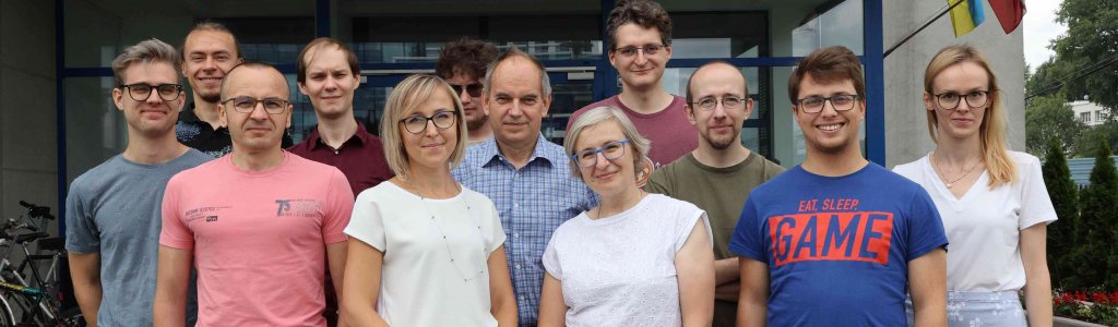
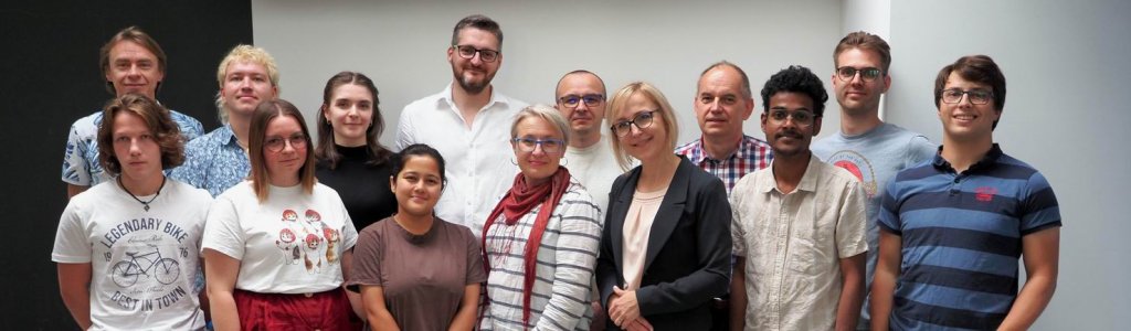
Our team
Skierbiszewski

Muzioł 
Turski 
Siekacz 
Sawicka 
Feduniewicz 
Nowakowski-Szkudlarek 
Wolny 
Hajdel 
Żak 
Chlipała, PhD, Eng. 
Gołyga 
Lach 
Peret-Malessa 
Nhaloor 
Parasar 
Jotwani

Projects
Current list of our projects:
1. VISSION
"Active building blocks for visible and near-infrared applications on a silicon nitride interposer"
2. SONATA - N-side
"Seizing the advantages of Nitrogen-polar GaN for III-nitride light emitters"
3. LIDER
"Towards yellow laser diodes with tunable InGaN pseudo-substrate relaxation enabled by nanoporous GaN"
4. OPUS - Single Photon Sources
"Single photon light-emitting diodes based on III-nitrides for quantum technologies"
5. PolArt
"Neuromorphic Polariton Accelerator”
6. DUVLas
"Deep ultraviolet laser diodes"
7. FirstTEAM
"Monolityczna integracja wielokolorowych matryc mikro- i nano-LEDów"
List of completed projects HERE
Gallery
Video (only Polish language version) recorded in 2014 - “Patent na Patent”:
From this short video you can learn about Grzegorz Muzioł PhD thesis (4:10). He explains the role of InGaN laser diode waveguide design on the optical mode leakage to GaN substrate (5:08). You can hear Prof. Czesław Skierbiszewski tellinng about the properties and applications of gallium nitride (3:25), and Prof. Piotr Perlin (TopGaN CTO) stressing the importance of innovative research for polish hi-tech business (8:34).
Contact
Address
Headquarter:
Institute of High Pressure Physics
Polish Academy of Sciences "UNIPRESS"
Sokołowska 29/37
01-142 Warsaw
MBE LAB location:
al. Prymasa Tysiąclecia 98
01-424 Warsaw
public transportation:
PKP Koło - tram stop
Obozowa - bus stop
Phones:
+48 22 8760351 - office
+48 22 8760324 - lab
E-mail:
czeslaw@unipress.waw.pl