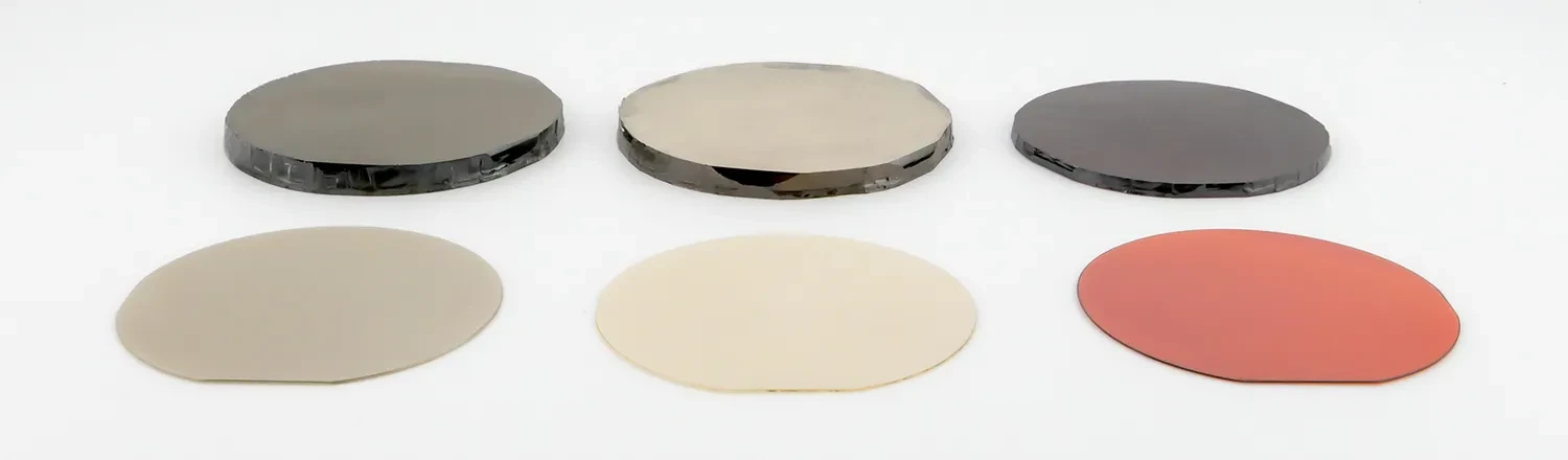
The Institute of High Pressure Physics of the Polish Academy of Sciences (IHPP PAS, UNIPRESS) offers ammonothermal GaN substrates produced on its pilot line. Dislocation density ranges from 103 cm−2 to 105 cm−2. Substrates are supplied with an epi-ready surface finish, ready for direct epitaxial growth. The offer includes substrates with various electrical properties and diameters of 1 inch and 2 inches.
On 8 January 2019 the Institute acquired Ammono S.A.; its commercial activity continues as the IHPP PAS pilot line, and substrates are delivered on demand.
Available types
- High n-type – high-carrier-concentration n-type
- Low n-type – low-carrier-concentration n-type (high transparency)
- Semi-insulating (SI) – semi-insulating
Sample substrates
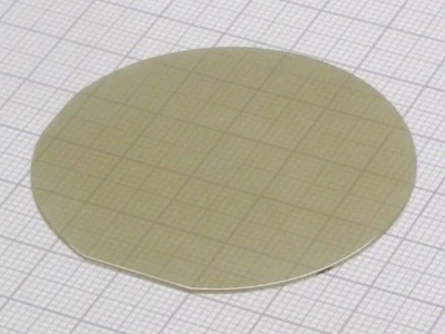
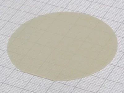
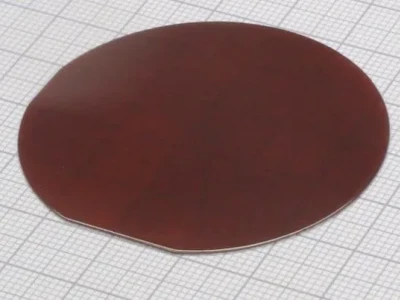
Prices and orders
The price of a substrate depends on its diameter and properties, such as orientation, selected misorientation angle and electrical parameters. To get a quote, please contact our sales department: sales@unipress.waw.pl.
To check whether a substrate with a non-standard specification can be ordered – e.g. a different crystallographic orientation, surface finish or thickness – please contact us directly.
High n-type – High-electron-concentration n-type, oxygen-doped
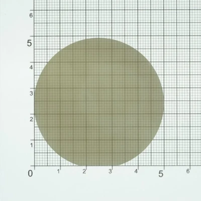
- Diameters: 1 inch, 2 inch
- Orientation: (0001) C plane
- Surface: epi-ready (RMS < 0.5 nm)
- Product codes: Cn0025-351-012-5-2-n100, Cn0050-351-082-5-2-n100
| Parameter | Unit | 1 inch | 2 inch |
|---|---|---|---|
| General specification | |||
| Orientation | (0001) C plane | (0001) C plane | |
| Thickness | µm | 350 (±50) | 430 (±50) |
| Dimensions | mm | Ø25.4 (±0.5) | Ø50.4 (±0.5) |
| Primary Flat (PF) | mm | 12 (±1) | 16 (±1) |
| Secondary Flat (SF) | mm | 8 (±1) | 8 (±1) |
| Bow | µm | 0 (±10) | 0 (±20) |
| Total Thickness Variation (TTV) | µm | ≤ 40 | ≤ 60 |
| Structural specification | |||
| Etch Pit Density (EPD) | cm⁻² | < 5 × 10⁴ | < 5 × 10⁴ |
| FWHM (0002) X-ray rocking curve, epi-ready surface, 100 × 100 µm slit | arcsec | ~ 20 | ~ 20 |
| Macrodefects | none | none | |
| Electrical specification | |||
| Conductivity type | n | n | |
| Carrier concentration | cm⁻³ | ~ 10¹⁹ | ~ 10¹⁹ |
| Resistivity | Ω·cm | ~ 10⁻³ | ~ 10⁻³ |
| Carrier mobility | cm²/V·s | ~ 150 | ~ 150 |
| Misorientation (measured at the centre of the substrate) | |||
| Deviation from the M plane | deg | 0 (±0.25) | |
| C plane – angle δ1 | deg | 0 (±0.20) | |
| C plane – angle δ2 | deg | ±0.5 (±0.20) | |
| Surface preparation | |||
| Front side | epi-ready polished (RMS < 0.5 nm) | ||
| Back side | ground | ||
Low n-type – Low-carrier-concentration (high-transparency) n-type, oxygen-doped
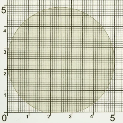
- Diameters: 1 inch, 2 inch
- Orientation: (0001) C plane
- Surface: epi-ready (RMS < 0.5 nm)
- Product codes: Cn0025-351-012-5-2-a100, Cn0050-351-082-5-2-a100
| Parameter | Unit | 1 inch | 2 inch |
|---|---|---|---|
| General specification | |||
| Orientation | (0001) C plane | (0001) C plane | |
| Thickness | µm | 350 (±50) | 430 (±50) |
| Dimensions | mm | Ø25.4 (±0.5) | Ø50.4 (±0.5) |
| Primary Flat (PF) | mm | 12 (±1) | 16 (±1) |
| Secondary Flat (SF) | mm | 8 (±1) | 8 (±1) |
| Bow | µm | 0 (±10) | 0 (±20) |
| Total Thickness Variation (TTV) | µm | ≤ 40 | ≤ 60 |
| Structural specification | |||
| Etch Pit Density (EPD) | cm⁻² | < 5 × 10⁴ | < 5 × 10⁴ |
| FWHM (0002) X-ray rocking curve, epi-ready surface, 100 × 100 µm slit | arcsec | ~ 20 | ~ 20 |
| Macrodefects | none | none | |
| Electrical specification | |||
| Conductivity type | n | n | |
| Carrier concentration | cm⁻³ | 2 × 10¹⁷ – 2 × 10¹⁸ | 2 × 10¹⁷ – 2 × 10¹⁸ |
| Resistivity | Ω·cm | 10⁻² – 10⁻¹ | ~ 10⁻² |
| Carrier mobility | cm²/V·s | ~ 200 – 250 | ~ 250 |
| Misorientation (measured at the centre of the substrate) | |||
| Deviation from the M plane | deg | 0 (±0.25) | |
| C plane – angle δ1 | deg | 0 (±0.20) | |
| C plane – angle δ2 | deg | ±0.5 (±0.20) | |
| Surface preparation | |||
| Front side | epi-ready polished (RMS < 0.5 nm) | ||
| Back side | ground | ||
Semi-insulating (SI) – semi-insulating, manganese-doped
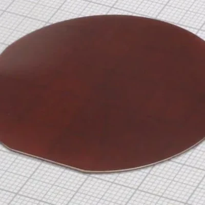
- Diameters: 2 inch
- Orientation: (0001) C plane
- Surface: epi-ready (RMS < 0.5 nm)
- Product codes: Cs0050-351-082-5-2-k200
| Parameter | Unit | 2 inch |
|---|---|---|
| General specification | ||
| Orientation | (0001) C plane | |
| Thickness | µm | 430 (±50) |
| Dimensions | mm | Ø50.4 (±0.5) |
| Primary Flat (PF) | mm | 16 (±1) |
| Secondary Flat (SF) | mm | 8 (±1) |
| Bow | µm | 0 (±20) |
| Total Thickness Variation (TTV) | µm | ≤ 60 |
| Structural specification | ||
| Etch Pit Density (EPD) | cm⁻² | < 5 × 10⁴ |
| FWHM (0002) X-ray rocking curve, epi-ready surface, 100 × 100 µm slit | arcsec | ~ 20 |
| Macrodefects | none | |
| Electrical specification | ||
| Conductivity type | SI | |
| Carrier concentration | cm⁻³ | — |
| Resistivity | Ω·cm | ≥ 10⁹ |
| Carrier mobility | cm²/V·s | — |
| Misorientation (measured at the centre of the substrate) | ||
| Deviation from the M plane | deg | 0 (±0.25) |
| C plane – angle δ1 | deg | 0 (±0.20) |
| C plane – angle δ2 | deg | ±0.5 (±0.20) |
| Surface preparation | ||
| Front side | epi-ready polished (RMS < 0.5 nm) | |
| Back side | ground | |
Type comparison
| Parameter | Unit | High n-type | Low n-type | Semi-insulating (SI) |
|---|---|---|---|---|
| Thickness | µm | 350 (±50) (1 inch) 430 (±50) (2 inch) | 350 (±50) (1 inch) 430 (±50) (2 inch) | 430 (±50) (2 inch) |
| Total Thickness Variation (TTV) | µm | ≤ 40 (1 inch) ≤ 60 (2 inch) | ≤ 40 (1 inch) ≤ 60 (2 inch) | ≤ 60 (2 inch) |
| Carrier concentration | cm⁻³ | ~ 10¹⁹ (1 inch) ~ 10¹⁹ (2 inch) | 2 × 10¹⁷ – 2 × 10¹⁸ (1 inch) 2 × 10¹⁷ – 2 × 10¹⁸ (2 inch) | — (2 inch) |
| Resistivity | Ω·cm | ~ 10⁻³ (1 inch) ~ 10⁻³ (2 inch) | 10⁻² – 10⁻¹ (1 inch) ~ 10⁻² (2 inch) | ≥ 10⁹ (2 inch) |
| Carrier mobility | cm²/V·s | ~ 150 (1 inch) ~ 150 (2 inch) | ~ 200 – 250 (1 inch) ~ 250 (2 inch) | — (2 inch) |
| Dopant | oxygen | oxygen | manganese | |
| Available diameters | 1 inch, 2 inch | 1 inch, 2 inch | 2 inch |
Structural parameters (EPD, FWHM), misorientation and surface preparation are common to all types.