-
Popularisation of science
- ⋅
- 14/04/2026
- ⋅
- Reading time approx. 2 min
Polska szkoła fizyki półprzewodników – od pionierskich badań do światowego znaczenia
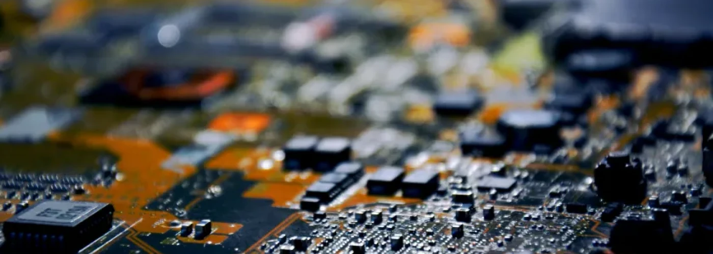
The presentation (in Polish) outlines the origins and development of the Polish school of semiconductor physics, initiated by Leonard Sosnowski - one of the pioneers of this field in Poland . Its beginnings date back to the 1940s, when semiconductor research was still emerging worldwide, particularly around the breakthrough discovery of the transistor in 1947.
A key role was played by Sosnowski’s research conducted in the United Kingdom, where early models of semiconductor junctions were developed and the photovoltaic effect in materials such as PbS was demonstrated. After returning to Poland, these studies laid the foundation for a new research field and for educating future generations of scientists.
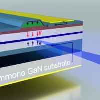
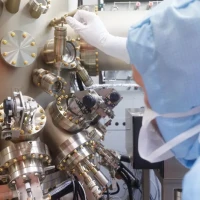
In the following decades, a strong scientific community was established around the Institute of Physics of the Polish Academy of Sciences and the University of Warsaw. Both theoretical and experimental research were intensively developed—from band structure and transport phenomena to advanced semiconductor material technologies . A particularly important achievement was the development of research on narrow bandgap semiconductors, which became a recognised Polish scientific specialisation.
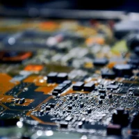
These efforts led to significant results, including discoveries related to band structure in materials such as HgTe, the development of theoretical models (e.g. the Kane model), and the construction of advanced semiconductor materials and detectors. This work contributed directly to the advancement of modern electronics, optoelectronics, and information technologies.
The presentation demonstrates how sustained fundamental research, strong scientific collaboration, and investment in research infrastructure led to the emergence of a globally recognised Polish school of semiconductor physics.
Downloads
 Presentation
 Latest